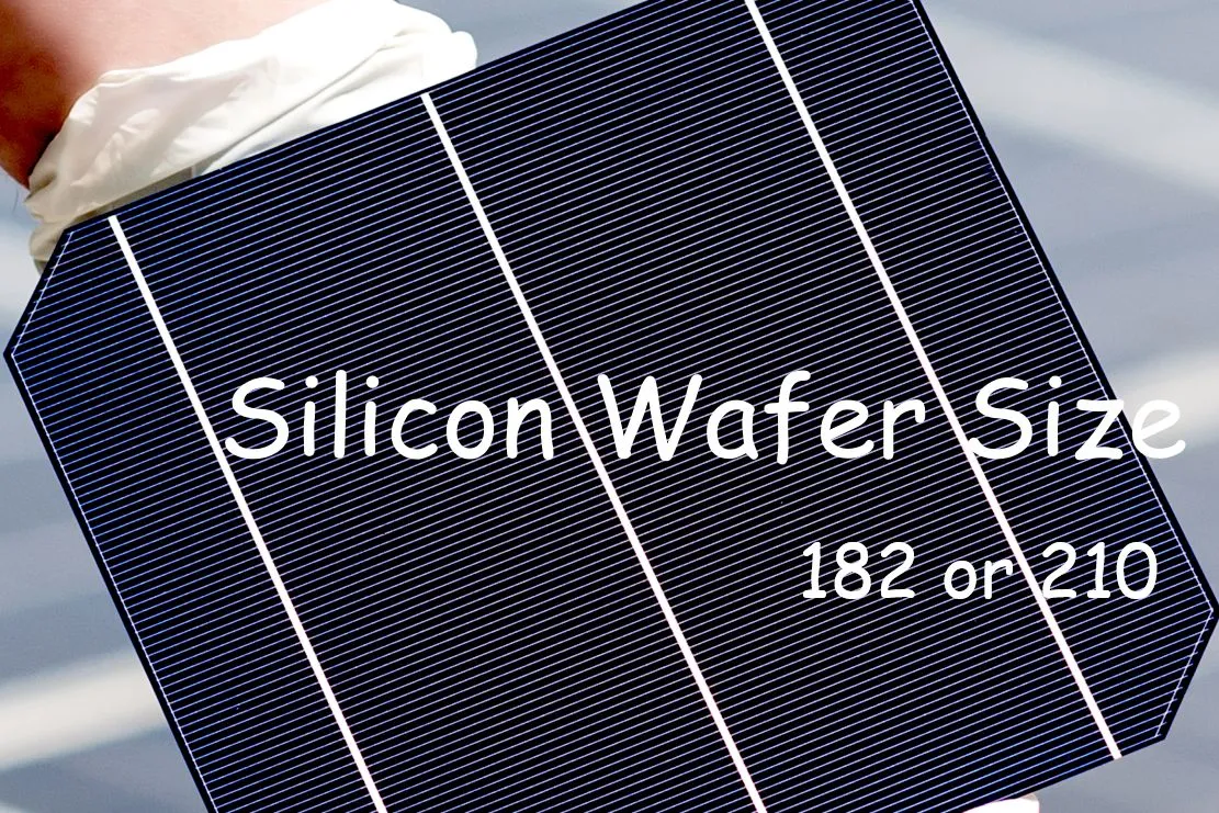
The photovoltaic industry is an innovative and competitive one, with wafer sizes changing as technology advances and markets expand. Currently, there are two main camps of silicon wafer sizes in the global PV industry, namely the 182 camp represented by Longi Green Energy, JinkoSolar, and JA Technology, and the 210 camp represented by Central, Trina Solar, and Rising East. Both camps advocate the advantages of large silicon wafers but disagree on the specific size selection. So, what are the respective advantages of these two camps? Which camp will dominate in the future? This article will explore these questions.
The formation of the 182 and 210 camps
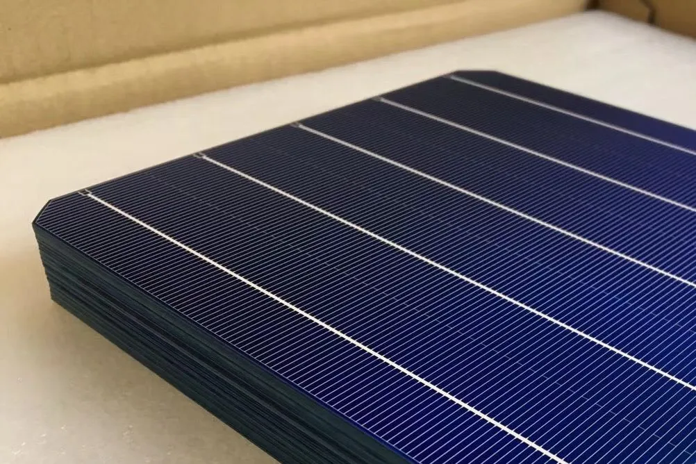
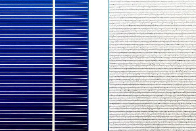
Silicon wafers are the core material of PV modules and their size directly affects the performance and cost of cells, modules, and systems. Over the past few decades, the size of silicon wafers has gradually grown from 100mm to 166mm. As market demand and technology advance, silicon wafer manufacturers have started to launch larger wafer-size products.
Many solar panel manufacturers such as Sungold also use monocrystalline cells of 166 and 210 for many of their products, as the difference in Silicon Wafer size makes a difference in the efficiency and appearance of the solar panels produced.
In 2019, LONGi Green Energy is the first to launch M6 wafers with a size of 166mm x 166mm, which can increase single wafer power and module power density and reduce system costs compared to the traditional 156mm x 156mm wafers. LONGi Green Energy believes that 166mm is the optimal wafer size because it can match existing cells, module equipment, and auxiliary materials to the greatest extent possible, reducing retrofit costs and technical difficulties.
In August of the same year, Zhonghuan launched its M12 wafer, which is 210mm x 210mm in size and can further increase single-wafer power and module power density and reduce system costs compared to the M6 wafer. Azeus believes that 210mm is the optimal wafer size as it can take advantage of semiconductor wafers, improve wafer quality and efficiency, and allow for one-step capacity expansion.
In June 2020, at SNEC, LONGi Green Energy launched another M10 wafer with a size of 182mm x 182mm. LONGi Green Energy said that after technical exploration, it found that 182mm was the largest size achievable with existing equipment and allowed for lower current, higher efficiency, and better compatibility. LONGi Green Energy has joined forces with JinkoSolar and JA Technology to form the M10 camp.
In November 2020, the Joint Initiative on Promoting Standardisation of 210mm Wafer and Module Sizes in the PV Industry was officially launched. The initiative was co-sponsored by Trina Solar, Rising East, Atos, Huan Sheng, Tongwei, RUNYANG, Zhonghuan, and Shangji NC. The initiative states that 210mm silicon wafers and modules are ready for large-scale production, which can bring higher cost performance and lower carbon emissions to the PV industry.
At this point, the global PV industry’s silicon wafer size camp has basically formed, with the 182 camps and the 210 camps representing two different technical routes and market strategies.

Advantages of the 182 and 210 camps
Both the 182 camp and the 210 camps have their own technical rationale and market strategies, specifically the following:
Advantages of the 182 camp
182 silicon wafers can match existing cell and module equipment to the greatest extent possible, reducing the cost and technical difficulty of retrofitting. It is reported that existing cell and module equipment can be adapted to 182 wafer production with only a small amount of retrofitting. This is a great advantage for integrated companies and stock capacity.
182 modules can be compatible with existing glass, back sheets, junction boxes, and other auxiliary materials to avoid capacity shortages and supply chain risks. It is noted that existing glass, back sheets, junction boxes, and other auxiliary materials can meet the needs of 182 modules without the need for large-scale replacement or upgrade. This is a great advantage in terms of ensuring the quality and stability of the modules.
182 modules can achieve lower currents, increased efficiency, and reduced hot spot temperature rise and internal consumption. The 182 modules is said to have a half-sheet design, which allows for lower currents, resulting in higher efficiency and lower hot spot temperature rise and internal consumption. This is a significant advantage in terms of improving the performance and lifetime of the module.
Advantages of the 210 camp
210 silicon wafers can achieve higher power per wafer, increasing module power density and reducing system costs. It is reported that 210 wafers can increase the power per wafer by approximately 10% compared to 182 wafers, thereby increasing module power density and reducing system costs. This is a significant advantage in meeting the market demand for higher-power modules.
The 210 module allows for lower voltages, increased string lengths, and a reduction in the number of DC cables and inverters. The 210 modules is said to have a three-split design, allowing for lower voltages, which increases string length and reduces the number of DC cables and inverters. This is a significant advantage in terms of reducing the balance of system (BOS) costs.
The 210 modules can take advantage of the semiconductor silicon wafers to improve wafer quality and efficiency. It is reported that 210 silicon wafers use the semiconductor-grade silicon wafer technology developed by Central, which has significant advantages in terms of grain size, grain boundary density, and oxygen content, thus improving wafer quality and efficiency. This is a great advantage for improving the performance and reliability of the modules.
New changes
In recent times, however, new changes have emerged in the PV industry. On the one hand, this is due to the continued rise in silicon prices, which has led to an increase in wafer costs and prompted wafer manufacturers to accelerate the process of thinning wafers in order to reduce silicon consumption and improve efficiency. On the other hand, it is due to the introduction of rectangular wafer products34 by some companies to make the most of the edge material around the silicon rods and to increase module power and efficiency. These changes have brought new shocks and challenges to the already stable wafer size pattern.
Rectangular wafers are wafers that extend in the length direction from the original square wafer and are available in a variety of sizes, such as 210182mm, 210191mm, 210*200mm, etc. The main advantage of rectangular wafers is that they can increase the power and efficiency of the module while making better use of silicon material and reducing the cost of the wafer. The main disadvantage of rectangular wafers is that they are less compatible with existing cell and module production lines and require investment in new production lines and equipment, making them more difficult to market.
At present, the market share of rectangular silicon wafers is not yet high, but it has already attracted widespread attention from the industry. Some companies have already started to launch rectangular wafer-based cells and modules, such as Trina Solar, which has launched a 2384*1134mm module, and Longi Green Energy, JinkoSolar, and JA Technology, which are also launching different modules using rectangular wafers. These products have brought new choices and challenges to downstream customers while increasing power and efficiency.
In the long term, the PV industry’s choice of wafer size should be aimed at the lowest cost per kWh, taking into account the synergistic development and resource efficiency of the upstream and downstream industry chain. Therefore, the unification and standardization of silicon wafer sizes is an inevitable trend in the industry’s development and is in the common interest of all parties. At present, the China Photovoltaic Industry Association (CPIA) is already actively promoting the standardization of silicon wafer sizes in the hope that a reasonable, scientific, and sustainable silicon wafer size specification can be formed as soon as possible to provide a guarantee for the healthy development of the PV industry.